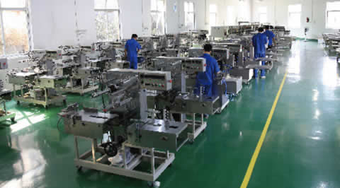
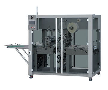
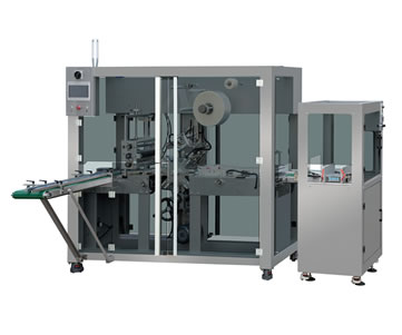
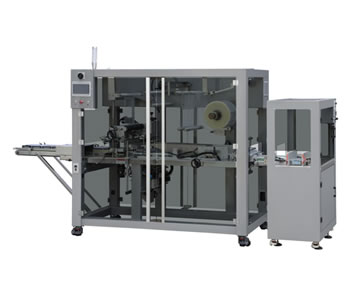
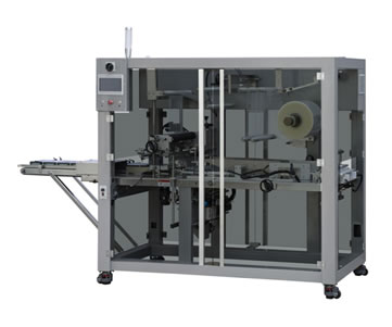
技術頻道

娓娓工業(yè)
您現在的位置: 中國傳動網 > 技術頻道 > 技術百科 > 英飛凌電源管理芯片TLF35584的使用介紹

英飛凌電源管理芯片TLF35584的使用介紹

時間:2024-03-12 13:55:18來源:嵌入式程序猿

導語:?TLF35584介紹

TLF35584是英飛凌推出的針對車輛安全應用的電源管理芯片,符合ASIL D安全等級要求,具有高效多電源輸出通道,寬電壓輸入范圍,根據不同的型號有3.3V和5.0V兩種命名。可以為MCU提供600mA的電源,可以提供200mA的電源給通信,還可以提供精確的參考電壓給ADC使用,具有SPI通信,可以監(jiān)控和配置該芯片。我們以TLF35584QVVS2型號的使用來做介紹。TLF35584的封裝類型以及電壓分類如下表所示:

TLF35584系統(tǒng)框圖

管腳介紹

PinSymbolFunction
1BSGBoost driver ground:
Connect this pin to ground at the low side of an external current sense resistorto
decouple the driver noise from the sensitive ground. If step up pre regulator option
is not used, connect to ground.
2VSTSupply voltage standby regulator, input:
Connect this input to supply (battery) voltage with reverse protection diodeand
capacitor between pin and ground. An EMCfilter is recommended.
3ENAEnable Input:
A positive edge signal at this pin will wake the device. In case of not used connect
to ground.
4WAKWake/Inhibit Input:
A high level signal of defined length at this pin will wake the device. In case of not
used, connect to ground
5QSTOutput standby LDO:
Connect a capacitor as close as possible to pin.
6AG1Analogue ground, pin 1:
Connect this pin directly (low ohmic and low inductive) to ground.
7AG2Analogue ground, pin 2:
Connect this pin directly (low ohmic and low inductive) to ground.
8AGS1Analogue ground, safety, pin 1:
Connect this pin directly (low ohmic and low inductive) to ground.
In case a safety switch is used, connect directly to the source of the NMOS used.
9AGS2Analogue ground, safety, pin 2:
Connect this pin directly (low ohmic and low inductive) to ground.
In case a safety switch is used, connect directly to the source of the NMOS used.
10SS2Safe state signal 2:
Safe state output signal 2, sets the application into a safe state. Signal is delayed against SS1, delay canbe adjusted via SPI command.
11SS1Safe state signal 1:
Safe state output signal 1, sets the application into a safe state.
12SDISerial peripheral interface, signal data input:
SPI signalling port, connect to SPI port “data output” of micro processor to receive commands during SPI communication.
13SDOSerial peripheral interface, signal data output:
SPI signalling port, connect to SPI port “data input” of micro processor to send
status information during SPI communication.
14SCLSerial peripheral interface, signal clock:
SPI signalling port, connect to SPI port “clock” of micro processor to clock the
device for SPI communication.
15SCSSerial peripheral interface, signal chip select:
SPI signalling port, connect to SPI port “chip select” of micro processor to address
the device for SPI communication.
16WDIWatchdog input, trigger signal:
Input for trigger signal, connect the “trigger signal output” of the micro processor to
this pin. In case of not used, leave open (internal pull-down).
17ROTReset output:
Open drain structure with internal pull-up current source. A low signal at this pin indicates a reset event.
18INTInterrupt signal:
Push-pull-stage. A low pulse at this pin indicates an interrupt, the micro processor shall read out the SPI status registers. Connect to a non maskable interrupt port (NMI) of the micro processor core supply voltage.
19SYNSynchronization output signal:
Connect this output to the optional external switch mode post regulator
synchronization input. The signal delivers the step down regulator switching
frequency either in phase or shifted by 180° (selectable via SPI command). The switch mode post regulator shall synchronize to the rising edge. If not used, leave open.
20ERRError signal input:
Input for error signal from micro processor safety managing unit (SMU, internal
failure detection of the micro processor). Connect the “error signal output” of the
micro processor to this pin.
21EVCEnable external post regulator for core supply:
Connect this pin to the enable input of the external post regulator. If not used, leave
open.
22MPSMicrocontroller programming support pin:
Pull down this pin to ground for operation. Optionally, this pin can be used for
microcontroller debugging and programming purposes. For details please refer to
Chapter 11.7.
23SECConfiguration pin for external post regulator for core supply:
Connect this pin to ground if the option external post regulator is not used. If the
option external post regulator is used, leave open.
24FREFrequency adjustment pin:
Connect pin to ground for low frequency range or leave open for high frequency
range.
25STUConfiguration pin for step up converter:
Connect this pin to ground if the option step up pre regulator is not used. If the
option step up pre regulator is used, leave open.
26VCIInput for optional external post regulator output voltage (core supply):
Connect an external resistor divider to adjust the over and under voltage
thresholds of reset output signal ROT.
If the option external post regulator is not used, leave open.
27GSTGate stress pin:
Not for customer use. Connect this pin directly (low ohmic and low inductive) to
ground.
28AG3Analogue ground, pin 3:
Connect this pin directly (low ohmic and low inductive) to ground.
29QVROutput voltage reference:
Connect a capacitor as close as possible to pin.
30QUCOutput LDO_uC supply (micro processor supply):
Connect a capacitor as close as possible to pin.
31QCOOutput LDO_communication supply:
Connect a capacitor as close as possible to pin.
32QT2Output tracker 2:
Connect a capacitor as close as possible to pin.
33QT1Output tracker 1:
Connect a capacitor as close as possible to pin.
34N.C.Internally not connected:
This pin is electrically not connected internally and can be kept open/floating,
connected to GND or any other signal. Consider neighboring signals for potential
failures.
46DRGDriver output for external step up regulator power stage, connect to gate:
Gate of low side switch of step up pre regulator: Connect to the gate of an external
N-channel mosfet, line to be straight and as short as possible. If step up pre
regulator option is not used, leave open.
47RSHSense resistor for external step up regulator power stage, high side:
Connect this pin to the high side of an external current sense resistor to determine
the maximum current threshold through the external N-channel mosfet. If step up
pre regulator option is not used, connect to ground.
48RSLSense resistor for external step up regulator power stage, low side:
Connect this pin to the low side of an external current sense resistor to determine
the maximum current threshold through the external N-channel mosfet. If step up
pre regulator option is not used, connect to ground.
EP1Edge pin no 1:
Keep area below this pin free of ground or other signals, do not solder this pin to
ground or any other signal. This pin must be kept free of soldering.

EP2Edge pin no 2:
Keep area below this pin free of ground or other signals, do not solder this pin to
ground or any other signal. This pin must be kept free of soldering.

EP3Edge pin no 3:
Keep area below this pin free of ground or other signals, do not solder this pin to
ground or any other signal. This pin must be kept free of soldering.

EP4Edge pin no 4:
Keep area below this pin free of ground or other signals, do not solder this pin to
ground or any other signal. This pin must be kept free of soldering.

Coolin
g Tab
GNDCooling Tab.
Connect externally to GND and heat sink area.

典型應用框圖

安全功能

TLF35584提供了很多安全功能來保證系統(tǒng)的安全

輸出電源軌監(jiān)控

Vprereg

VQUC

VQST

VQVR

VVCI

VQT1, VQT2

VQCO

提供MCU外部安全機制的時序時間監(jiān)控服務

監(jiān)控MCU的SMU ERR輸出功能

監(jiān)控MCU的看門狗輸出服務

二次安全關斷能力

TSR

TSR01 -在所有產生和監(jiān)控的輸出電壓上檢測和響應故障。違反將會導致系統(tǒng)級的單點失效

TSR02 -檢測并響應MCU安全管理單元(SMU)的錯誤觸發(fā)。違反會導致潛伏失效或者多點失效

TSR03 -檢測并響應由MCU錯誤觸發(fā)的定時監(jiān)控服務,違反會導致潛伏失效或者多點失效

TSR04 -內部需要時激活二次關斷信號,違反TSR04可能會導致潛伏失效

安全功能應用

安全路徑

安全路徑是信號鏈和電路使能并維持系統(tǒng)的安全狀態(tài)。對于一些TLF35584目標應用,達到了安全狀態(tài)

通過禁用執(zhí)行器、通信通道或整個系統(tǒng)。在這樣的系統(tǒng)中,安全路徑是安全停機路徑。

首要安全路徑

主要安全路徑不是由PMIC管理的,而是由MCU單片機控制的。因此,主安全路徑不依賴于PMIC的安全邏輯。通常,這類安全路徑是通過安全MCU建立的。該單片機可以使應用程序始終處于安全狀態(tài),使用的條件在有效范圍內,外部安全機制可用。

二次安全路徑

二次安全路徑或者叫二次關斷路徑是通過PMIC的安全功能實現的。在PMIC的安全功能TSR需求中,系統(tǒng)的安全狀態(tài)是通過PMIC的安全狀態(tài)輸出達到的,也就是說通過TLF35584的SS1和SS2輸出連接到系統(tǒng)電路可以釋放或者進入安全狀態(tài),這種機制可以在檢測到關鍵失效時候進入安全狀態(tài)已達到安全目標。

安全狀態(tài)

系統(tǒng)的安全狀態(tài)被認為是沒有任何不合理的高水平風險的運行模式

Assumption:[SM_00_01]

只要TLF35584處于安全狀態(tài)(通過激活二次安全關機路徑,即SS1/SS2處于低電平表示),則子系統(tǒng)處于安全狀態(tài)。

TLF35584包括許多安全設計功能和安全機制,以支持實現技術安全分析總結報告中定義的安全級別的安全要求.

安全特性

安全特性概覽

安全特性如下圖中標紅色部分所示

輸出電壓監(jiān)控

TLF35584為所有輸出提供了獨立的電源監(jiān)控功能,每一路輸出都包含獨立的過壓和欠壓監(jiān)控

帶隙基準和內部電壓監(jiān)控

所有的內部電壓也會被監(jiān)控,如果出現異常會進入POWNDOWN狀態(tài)。TLF35584包含兩路互相獨立的帶隙基準參考電壓互相監(jiān)控對方的操作。如果超過某一預設的門限值,TLF35584將會產生一個中斷給到外部,MCU可以利用這個中斷做一些響應。

熱關斷

TLF35584包含熱監(jiān)控以保護設備在高溫條件下損壞,內部有多點的溫度保護來防止器件損壞,如果檢測到過溫,會產生中斷給到MCU, MCU應當作出一些反映,如可以關斷某路電源輸出。

錯誤管腳監(jiān)控

TLF35584提供一個可以通過ERR腳監(jiān)控MCU的安全管理單元SMU,一個預定義的頻率范圍的翻轉方波信號必須給到TLF35584的ERR腳,如果是超過頻率范圍的信號給到ERR腳會引起報故障,TLF35584將會進入INT狀態(tài)。默認情況下ERR腳功能是使能的。

窗口看門狗

TLF35584包含一個窗口看門狗來監(jiān)控MCU的運行,需要一定間隔內收到觸發(fā)信號,可以通過WDI腳或者SPI,在一定的開窗時間內或者超時觸發(fā)都會被認為是無效的看門狗觸發(fā),無效看門狗觸發(fā)事件將會引起內部錯誤計數器加2,并且產生中斷,有效的看門狗觸發(fā)事件將會引起錯誤計數減1,如果錯誤計數器超過配置的門限值,TLF35584將會跳轉到INT狀態(tài)。默認條件下窗口看門狗是使能的,需要注意的是窗口看門狗和功能看門狗是相互獨立的,可以同時使能使用。

功能看門狗

功能看門狗稍微復雜一些,也叫問答看門狗,通過多個SPI通信幀完成。TLF35584產生一個問題,同時心跳計數器開始從0向上計數,直到心跳周期結束,心跳周期可以通過SPI調整配置,4個字節(jié)的響應答案必須在心跳周期結束之前收到。最后一個收到的響應必須同步寫入同步寄存器以復位心跳計數器。如果接收到正確的答案響應,認為是一次有效的看門狗觸發(fā)事件,有效的看門狗觸發(fā)事件會導致內部錯誤計數器減1,無效的看門狗觸發(fā)事件將會導致內部錯誤計數器加2,并且產生中斷。如果錯誤計數器超過預設的門限值,將會跳轉到INT狀態(tài)。默認情況下功能看門狗是禁止的,和窗口看門狗可以獨立使用,互不干涉。

二次安全關斷能力

TLF35584具有二次安全關斷能力,在應用中安全狀態(tài)輸出引腳SS1和SS2的狀態(tài)用來表明設備的安全狀態(tài)。

軟錯誤檢測和修正

TLF35584通過一些寄存器提供了軟錯誤的檢測和修正安全機制,包括單個位錯誤的檢測和修正,以及兩個位錯誤的檢測。兩個位錯誤會引起中斷。

安全機制軟件需求

TLF35584在安全相關應用中用作微處理器電源。安全機制必須由相應的微處理器執(zhí)行,以保證系統(tǒng)的正確運行。

SPI通信

來自微處理器的SPI通信用于配置TLF35584,服務看門狗和監(jiān)控狀態(tài)寄存器,由于SPI通信是用來傳輸安全相關信息的,因此需要采取措施保證其數據的完整性

奇偶校驗

Assumption: [SM_SPI_01]

SPI通信中的奇偶校驗位為每次通信進行檢查。具有無效奇偶校驗信息的數據必須被忽略。

奇偶校驗位在SPI期間防止單比特故障和奇數比特錯誤的故障溝通。為了提供更全面的誤差覆蓋范圍,可以考慮額外的措施。如果在讀操作過程中奇偶校驗信息不正確,微處理器必須忽略數據和重做讀操作

如果寫操作過程中的校驗信息不正確,TLF35584將忽略該數據并產生中斷。微處理器應該響應中斷并檢查中斷源,即檢查是否SPI.PARE位置位。如果寫操作失敗,微處理器應該重復這個操作。

配置

Assumption: [SM_SPI_02]

write-verify-apply過程用于對安全相關配置的寫訪問。因此,數據應是在寫入數據之后和應用于應用程序之前進行驗證。預期配置的驗證至少每次配置校驗一次,并根據應用程序可以重新配置。

所有與安全相關的配置寄存器(稱為“受保護的寄存器”)都由定義的LOCK/UNLOCK過程,允許在數據激活之前對其進行驗證。

清除狀態(tài)和中斷寄存器

所有狀態(tài)和中斷標志在清除之前被正確讀取。掛起的中斷沒有正確清除服務

中斷信號

Assumption: [SM_INT_01]

根據具體的應用,在將中斷信號用作安全功能的應用中,對每個中斷信號的正確功能進行驗證。

中斷的處理,當產生中斷,應遵循:

可以實施超時,其到期應視為測試失敗。持續(xù)時間超時時間應根據所選擇的中斷源設置

讀取中斷狀態(tài)寄存器并驗證中斷標志是否與生成的特定中斷相匹配

中斷響應

Assumption: [SM_INT_02]

微處理器檢查每個中斷事件的中斷源,并根據應用程序做出反應要求。

Assumption: [SM_INT_03]

如果通過中斷狀態(tài)標志SYSSF.CFGE檢測到一個配置錯誤,MCU應該對設備進行重新配置

復位輸出使用

Assumption: [SM_ROT_01]

TLF35584的復位輸出腳ROT連接到MCU的復位輸入引腳,當有復位引腳輸出,主要安全路徑激活。

備用Stand-by LDO使用

Assumption: [SM_SBL_01]

在備用LDO用作微控制器的存儲器電源供給時,需要每個周期確認驗證下此LDO是否安全。

獨立的二次安全關斷路徑

Assumption: [SM_SS_01]

必須確保主要安全關斷路徑和二次安全關斷路徑的獨立性,不能存在任何的依賴關系。

一次關斷路徑或者腳主要關斷路徑由MCU控制。

Assumption: [SM_SS_02]

在將二次關斷路徑用作安全功能的應用中,根據不同的應用,要驗證其正確的功能,每個周期至少需要一次安全功能驗證。

窗口看門狗

Assumption: [SM_WWD_01]

在將窗口看門狗用作安全功能的應用程序中,根據應用至少在每個駕駛周期驗證一次窗口看門狗的正確性

Assumption: [SM_WWD_02]

在將窗口看門狗用作安全功能的應用程序中,其正確的功能包括微處理器復位信號ROT和安全狀態(tài)輸出的激活在每個周期至少驗證一次。

功能看門狗

Assumption: [SM_FWD_01]

在將功能看門狗用作安全功能的應用中,至少要驗證其正確的功能,每個駕駛周期一次,取決于應用程序。

Assumption: [SM_FWD_02]

在功能看門狗作為安全功能發(fā)布的應用程序中,其正確的功能包括微處理器復位信號ROT和安全狀態(tài)輸出的激活在每次駕駛中至少驗證一次,周期取決于應用程序。

ERR引腳監(jiān)控

Assumption: [SM_ERR_01]

在將ERR引腳用作安全功能的應用程序中,每次至少驗證一次其正確功能,驅動周期取決于應用。

Assumption: [SM_ERR_02]

在ERR引腳用作安全功能的應用中,其正確的功能包括微處理器復位信號ROT和安全狀態(tài)輸出的激活在每個駕駛周期至少驗證一次。

請注意,測試程序的可用性取決于錯誤引腳監(jiān)控的配置應用:立即行動與恢復延遲

監(jiān)控組件

Assumption: [SM_MON_01]

在監(jiān)控塊用作安全功能的應用程序中,監(jiān)視器的正確功能,每個使用的監(jiān)視器每個驅動周期至少驗證一次對中斷信號的監(jiān)控。

Assumption: [SM_MON_02]

在監(jiān)控塊用作安全功能的應用程序中,監(jiān)視器的正確功能在對每個已使用的監(jiān)視器至少進行一次驗證,以激活安全狀態(tài)輸出周期取決于應用程序。

ABIST

ABIST的檢測由MCU發(fā)起請求

詳細執(zhí)行規(guī)則可以參考SM手冊要求,這里不在贅述。

監(jiān)控功能恢復

如果對設備的監(jiān)督功能的測試導致異常或失敗,則相應的監(jiān)督功能應被認為是非活性的,并應考慮相應的系統(tǒng)反應以確保安全操作。由于缺乏監(jiān)督功能并不一定意味著違反了安全目標,微控制器可以控制場景,以增加系統(tǒng)的可用性。進一步講系統(tǒng)集成者可以預見恢復機制,使監(jiān)管恢復有效運作。,如可以重新配置有問題的配置,或者重啟TLF35584.

硬件需求

二次關斷路徑

Assumption: [SM_SS_03]

在應用中要確保SS1和SS2的高電平輸出被認為是使二次安全關斷路徑無效,低電平或者高阻態(tài)被認為是激活安全關斷路徑的信號。

Assumption: [SM_SS_04]

SS1和SS2之間的延遲不能被視為安全特性

最大額定值

Assumption: [SM_ABS_01]

在任何操作下都不能違反數據手冊中電氣參數的最大額定值

電壓電流

溫度

外部器件的選擇

反相保護

因為TLF35584本身不能夠處理反相供電的情況,所以需要外部系統(tǒng)層的額外電路來處理電池電壓的反接情況。

輸入濾波

為了使TLF35584都在額定電氣參數范圍內操作,強烈建議添加輸入濾波器,以限制電源線上的尖峰,相關的參數可以從TLF35584的EMC測試報告中獲取。

過流限制

強烈建議在管腳添加限流電阻,防止引腳的電流超過手冊的限制值。輸入電壓VST的限制主要靠前級降壓器件來提供可靠輸入。如我們的應用中的LM5085.

主要分為兩類

一類是連接到電池電壓等級的ENA和WAK腳必須小心處理過流和反相,至少大于10K的串聯電阻

第二類是像SPI(SCS,SCL,SDI,SDO),INT,ROT,WDI,SYN,EVC 至少串聯一個大于50歐姆的電阻,電阻布局的位置也需在系統(tǒng)級考慮。

ERR腳保護

在MCU的SMU故障輸出腳P33.8和TLF35584的ERR腳之間串聯大于1K的電阻。

電壓域的分離

強烈建議將ECU內的高、低壓區(qū)分開,在不同組的信號之間的電路以減少短路的風險。這可以通過在PCB布線中使用足夠的間隙來完成任何外部高壓和內部低壓信號之間。在這種情況下應給予特別考慮不同域的信號在引腳上連接。

外部被動元器件

必須強制確保連接到TLF35584的外部器件在數據手冊要求的范圍內,如輸出電感,電容等。外部器件組件的失效必須在系統(tǒng)層級覆蓋,可以使用冗余外部器件,提高系統(tǒng)層級的可靠性??梢詤⒖紨祿謨杂嘘P外部器件要求更詳細的信息,這里只給出簡單的要求

總結:

要根據自己的應用選擇內外安全機制去執(zhí)行,提高系統(tǒng)的安全。


標簽: 芯片

點贊

分享到:

上一篇:采煤機用牽引干式變壓器優(yōu)化...

下一篇:機器人底座的作用及種類有哪些?

中國傳動網版權與免責聲明:凡本網注明[來源:中國傳動網]的所有文字、圖片、音視和視頻文件,版權均為中國傳動網(www.treenowplaneincome.com)獨家所有。如需轉載請與0755-82949061聯系。任何媒體、網站或個人轉載使用時須注明來源“中國傳動網”,違反者本網將追究其法律責任。

本網轉載并注明其他來源的稿件,均來自互聯網或業(yè)內投稿人士,版權屬于原版權人。轉載請保留稿件來源及作者,禁止擅自篡改,違者自負版權法律責任。

網站簡介|會員服務|聯系方式|幫助信息|版權信息|網站地圖|友情鏈接|法律支持|意見反饋|sitemap

中國傳動網-工業(yè)自動化與智能制造的全媒體“互聯網+”創(chuàng)新服務平臺

網站客服服務咨詢采購咨詢媒體合作

Chuandong.com Copyright ?2005 - 2024 ,All Rights Reserved 版權所有 粵ICP備 14004826號 | 營業(yè)執(zhí)照證書 | 不良信息舉報中心 | 粵公網安備 44030402000946號